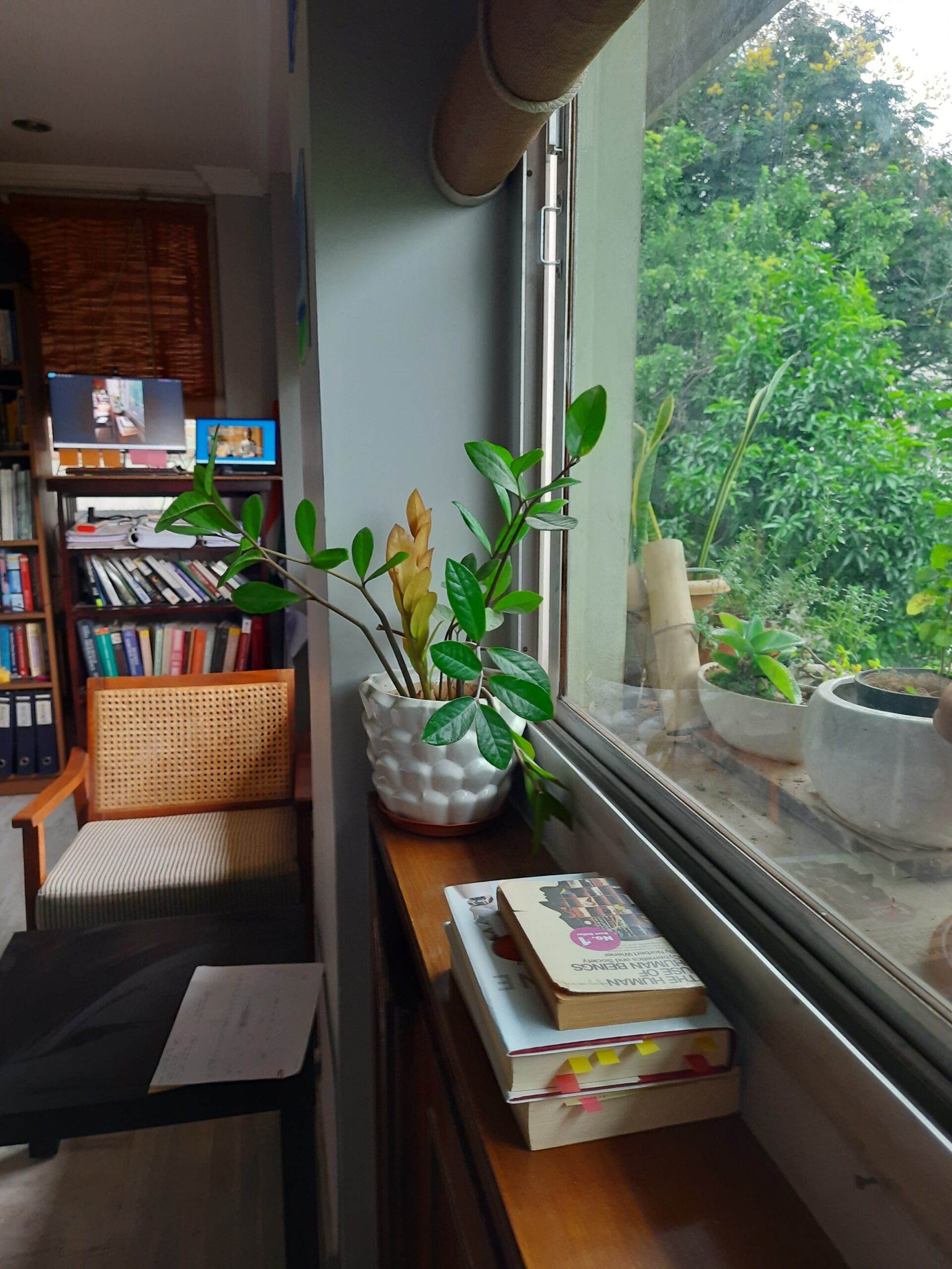
Making our own printed circuit board is a process which involves making libraries of various components identified for the design, constructing a schematic by connecting those components together and then verifying if all the design connections meet the design rules. Once the schematic meets the design rules, a file is generated that contains all the component information and interconnection details which is used to make a layout for the pcb.
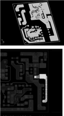
For designs with such feedback loops are involved this phase of laying out the circuit for fabrication is crucial. Though the overall design might seem simple, yet this phase could mean a lot in terms of the products performance and reliability.
Considering my longer-term plan and line up of products in the pipeline, I had invested in purchasing a license for an ECAD tool.
Per my recollection there was a key anniversary for the tool vendor who gave us a good deal with some additional packages (signal integrity, etc.) that would turn out to be useful on some of the other products we developed later in our journey.
The team that I had was not skilled to do the laying out part of the design, so I had to take help from a part time employee to do that.
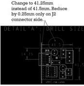
Normally, I have seen some layout engineers who get really annoyed for any kind of changes after giving the original design files. But this person was very flexible and patiently accommodated our iterative change requests. We later became good friends.
After the laying out of the circuit is completed, we normally generate a few files to be shared with the pcb fabricator. The files are called gerber files. Before finalizing the files for fabrication, we had to make sure the mechanical dimensions were in line with the enclosure being designed. Since we did not have the 3D CAD model available, yet we made a paper box type enclosure that was a replica of the mechanical enclosure design that we were trying to get developed. We cut out a few thick paper in the size of the PCB as well and checked if that would fit in the box.
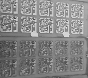
The pcb fabricator uses these files to create a photo mask on a copper clad sheet. This is normally done by printing each layer Gerber file on a transparent plastic sheet (film) and later super imposing the image onto a copper clad sheet using Ultra Voilet rays. This masked copper sheet is placed in a etching chemical, typically Ferric Chloride
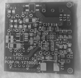
which etches out all copper except for the masked portion. The finished output is an etched sheet with connections traces between points. This process is repeated for each layer. Once all the layers are etched all of them are stacked

on over the other and heat laminated. This forms the final printed circuit board. The process is a little more complex for high density designs, but the principle is still the same.
We also shared the drill file which tells the fabricator where to drill holes on the pcb. These holes serve various purposes including where to place components and connectors.
In more complex designs with high part count there are other files also like x-y coordinate files which are used as inputs to a machine that does the placement of components automatically.
In this case, since the component count was less and our volumes also were low, we did not have the need to go for automated machine-based component assembly.
Again, through some contact I bounced around multiple PCB manufacturers and end up with one manufacturer, who was kind enough to manufacture our design in a short time even though we were a small company. We received the proto boards in around three to four days. After the basic inspection we assembled our components. We managed to solder the bigger
components ourselves but for the finer IC pins we requested a part time soldering technician to help us out. Finally, we had our own first fully assembled circuit board ready for testing.
